Microprocessor of TU IT Assistant
Microprocessor
A Microprocessor is a programmable device that takes in input, performs some arithmetic and logical operations over it and produces the desired output. In simple words, a Microprocessor is a digital device on a chip that can fetch instructions from memory, decode and execute them, and give results. It is an important part of a computer architecture without which you will not be able to perform anything on your computer.
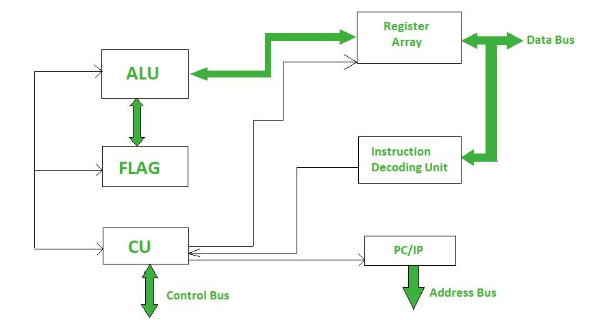
Block Diagram of a Microprocessor
A Microprocessor takes a bunch of instructions in machine language and executes them, telling the processor what it has to do. The microprocessor performs three basic things while executing the instruction:
It performs some basic operations like addition, subtraction, multiplication, division, and some logical operations using its Arithmetic and Logical Unit (ALU). New Microprocessors also perform operations on floating-point numbers.
Data in microprocessors can move from one location to another.
It has a Program Counter (PC) register that stores the address of the next instruction based on the value of the PC, Microprocessor jumps from one location to another and makes decisions.
A typical Microprocessor structure looks like this.
Applications of Microprocessor
Given below are the Applications of the Microprocessors
Computer: The Microprocessors are the CPU's in computers.
Embedded Systems: It is utilized as the main processing block in the Embedded systems such as Washing machines, microwaves and other equipments.
Industrial Automation: It can be used to control Industrial machinery and equipments.
Automotive: The Modern day Vehicles uses Microprocessors in there ECUs.
Telecommunications: The Microprocessors are utilized in the Telecommunications systems such as routers, modems, and switches.
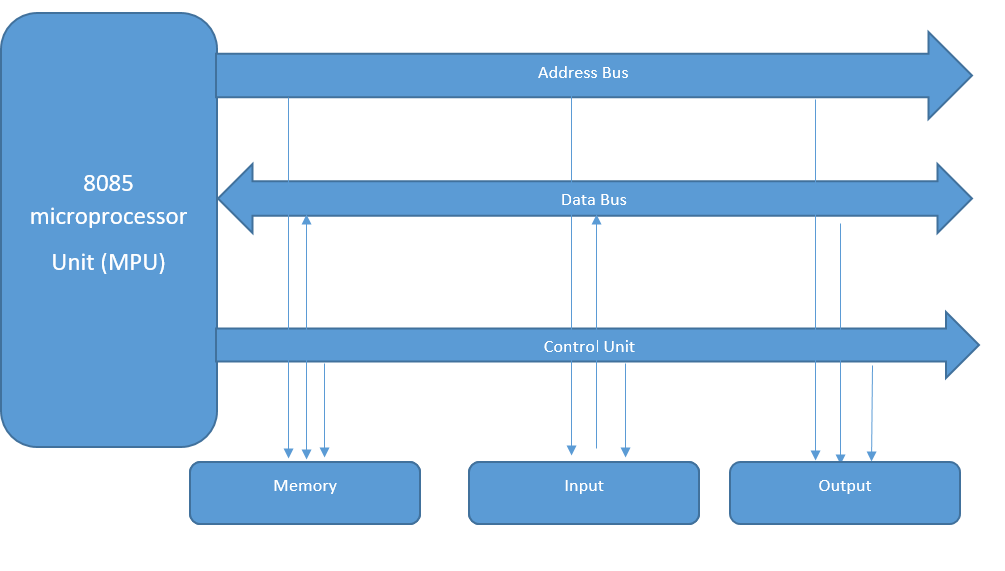
Bus System of Microprocessor Based System /Bus Organization
A bus organization is a group of conducting wires which carries information, all the peripherals are connected to microprocessor through the bus. A system bus is nothing just a group of wires to carry bits.
The MPU (Micro Processing Unit) performs primarily four operations:
Memory Read: Read data (or instructions) from memory.
Memory Write: Write data (or instructions) into memory.
I/O Read: Accepts data from I/P devices.
I/O Write: Sends data to O/P devices.
The diagram to represent the bus organization of 8085 microprocessor is given below:-
Types of Bus in the microprocessor are:-
Address Bus
Data Bus
Control Bus
i. Address Bus:-
The address bus carries information about the location of data in the memory. The addresses bus is unidirectional because of data flow in one direction, from the microprocessor to memory or from the microprocessor to input/out devices. Length of Address bus of 8085 microprocessor is 16 bit (That is, four hexadecimal digits), ranging from 0000H to FFFF H. The microprocessor 8085 can transfer maximum 16-bit address which means it can address 65,536 different memory location i.e 64KB memory.
Address Bus is used to perform the first function, identifying a peripheral or a memory location.
ii. Data Bus:-
The data bus allows data to travel between the microprocessor (CPU) and memory (RAM). The data bus is bidirectional because of data flow in both directions, from the microprocessor to memory or input/output devices and from memory or input/output devices to microprocessors. Length of Databus of 8085 microprocessor is 8 bit (that is, two hexadecimal Digits0, ranging from 00H to FF H.
The data bus is used to perform the second function, transferring binary information.
iii. Control Bus:-
The control bus carries the control signals to control all the associated peripherals, the microprocessor uses control bus to process data, that is what to do with selected memory location signals are:-
a. memory card
b.memory write
c. input/output,write.
Intel 8085 microprocessor architecture
A microprocessor is fabricated on a single integrated circuit (IC) or chip that is used as a central processing unit (CPU).The 8085 microprocessor is an 8-bit microprocessor that was developed by Intel in the mid-1970s. It was widely used in the early days of personal computing and was a popular choice for enthusiasts due to its simplicity and ease of use. The architecture of the 8085 microprocessor consists of several key components, including the accumulator, registers, program counter, stack pointer, instruction register, flags register, data bus, address bus, and control bus.
The accumulator is an 8-bit register that is used to store arithmetic and logical results. It is the most commonly used register in the 8085 microprocessor and is used to perform arithmetic and logical operations such as addition, subtraction, and bitwise operations.
Features of 8085 Microprocessor
The 8085 microprocessor has six general-purpose registers (B, C, D, E, H, and L), which can be paired as BC, DE, and HL for 16-bit operations.
The program counter (PC) is a 16-bit register that holds the address of the next instruction and increments after each instruction execution.
The stack pointer (SP) is a 16-bit register that keeps track of the top of the stack, used for storing return addresses and temporary data.
The instruction register is an 8-bit register that holds the instruction currently being executed.
The flags register is an 8-bit register that stores status flags, including Carry (set when an arithmetic operation generates a carry), Zero (set when the result is zero), Sign (set when the result is negative), and Parity (set when the result has an even number of 1s).
The data bus is an 8-bit bidirectional bus that transfers data between the microprocessor and memory or other devices.
The address bus is a 16-bit unidirectional bus that specifies memory locations and devices the microprocessor accesses.
The control bus consists of signals that manage microprocessor operations, including Read (to fetch data), Write (to store data), Interrupt (to signal an external event), and Reset (to restart the microprocessor).
8085 is an 8-bit, general-purpose microprocessor. It consists of the following functional units:
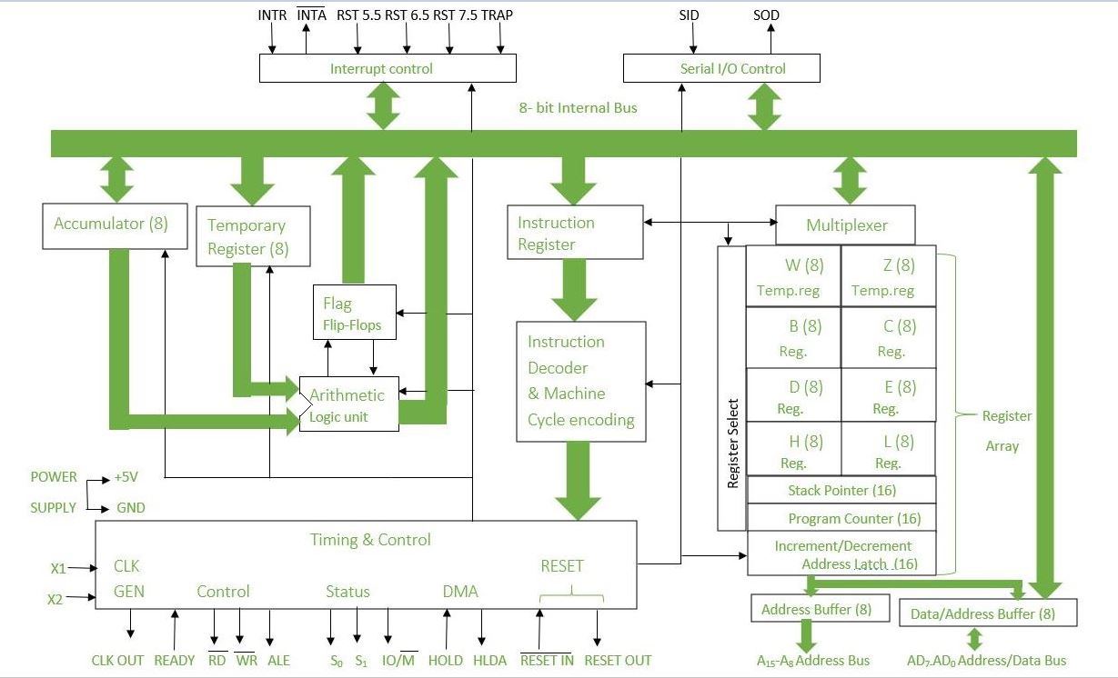
Arithmetic and Logic Unit (ALU)
It is used to perform mathematical operations like addition, multiplication, subtraction, division, decrement, increment, etc. Different operations are carried out in ALU: Logical operations, Bit-Shifting Operations, and Arithmetic Operations.
Flag Register
It is an 8-bit register that stores either 0 or 1 depending upon which value is stored in the accumulator. Flag Register contains 8-bit out of which 5-bits are important and the rest of 3-bits are “don’t Care conditions”. The flag register is a dynamic register because after each operation to check whether the result is zero, positive or negative, whether there is any overflow occurred or not, or for comparison of two 8-bit numbers carry flag is checked. So for numerous operations to check the contents of the accumulator and from that contents if we want to check the behavior of given result then we can use Flag register to verify and check. So we can say that the flag register is a status register and it is used to check the status of the current operation which is being carried out by ALU.
Different Fields of Flag Register
Carry Flag
Parity Flag
Auxiliary Carry Flag
Zero Flag
Sign Flag
Accumulator
Accumulator is used to perform I/O, arithmetic, and logical operations. It is connected to ALU and the internal data bus. The accumulator is the heart of the microprocessor because for all arithmetic operations Accumulators’ 8-bit pin will always there connected with ALU and in most-off times all the operations carried by different instructions will be stored in the accumulator after operation performance.
General Purpose Registers
There are six general-purpose registers. These registers can hold 8-bit values. These 8-bit registers are B,C,D,E,H,L. These registers work as 16-bit registers when they work in pairs like B-C, D-E, and H-L. Here registers W and Z are reserved registers. We can’t use these registers in arithmetic operations. It is reserved for microprocessors for internal operations like swapping two 16-bit numbers. We know that to swap two numbers we need a third variable hence here W-Z register pair works as temporary registers and we can swap two 16-bit numbers using this pair.
Program Counter
Program Counter holds the address value of the memory to the next instruction that is to be executed. It is a 16-bit register.
For Example: Suppose current value of Program Counter : [PC] = 4000H
(It means that next executing instruction is at location 4000H.After fetching,program Counter(PC) always increments by +1 for fetching of next instruction.)
Stack Pointer
It works like a stack. In stack, the content of the register is stored that is later used in the program. It is a 16-bit special register. The stack pointer is part of memory but it is part of Stack operations, unlike random memory access. Stack pointer works in a continuous and contiguous part of the memory. whereas Program Counter(PC) works in random memory locations. This pointer is very useful in stack-related operations like PUSH, POP, and nested CALL requests initiated by Microprocessor. It reserves the address of the most recent stack entry.
Temporary Register
It is an 8-bit register that holds data values during arithmetic and logical operations.
Instruction register and decoder
It is an 8-bit register that holds the instruction code that is being decoded. The instruction is fetched from the memory.
Timing and Control Unit
The timing and control unit comes under the CPU section, and it controls the flow of data from the CPU to other devices. It is also used to control the operations performed by the microprocessor and the devices connected to it. There are certain timing and control signals like Control signals, DMA Signals, RESET signals and Status signals.
Interrupt Control
Whenever a microprocessor is executing the main program and if suddenly an interrupt occurs, the microprocessor shifts the control from the main program to process the incoming request. After the request is completed, the control goes back to the main program. There are 5 interrupt signals in 8085 microprocessors: INTR, TRAP, RST 7.5, RST 6.5, and RST 5.5.
Priorities of Interrupts: TRAP > RST 7.5 > RST 6.5 > RST 5.5 > INTR
Address Bus and Data Bus
The data bus is bidirectional and carries the data which is to be stored. The address bus is unidirectional and carries the location where data is to be stored.
In the 8085 microprocessor, the address bus and data bus are two separate buses that are used for communication between the microprocessor and external devices.
The Address bus is used to transfer the memory address of the data that needs to be read or written. The address bus is a 16-bit bus, allowing the 8085 to access up to 65,536 memory locations.
The Data bus is used to transfer data between the microprocessor and external devices such as memory and I/O devices. The data bus is an 8-bit bus, allowing the 8085 to transfer 8-bit data at a time. The data bus can also be used for instruction fetch operations, where the microprocessor fetches the instruction code from memory and decodes it.
The combination of the address bus and data bus allows the 8085 to communicate with and control external devices, allowing it to execute its program and perform various operations.
Serial Input/Output Control
It controls the serial data communication by using Serial input data and Serial output data.
Serial Input/Output control in the 8085 microprocessor refers to the communication of data between the microprocessor and external devices in a serial manner, i.e., one bit at a time
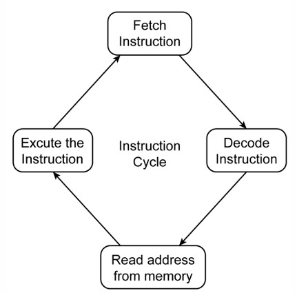
Instruction Cycle
A program consisting of the memory unit of the computer includes a series of instructions.
The program is implemented on the computer by going through a cycle for each instruction.
• The instruction cycle (also known as the Fetch–Decode–Execute cycle or the fetch-execute cycle) is the basic operational process of a computer system.
• The time taken for the execution of an instruction is known as the Instruction Cycle.
• It is the process by which a computer retrieves a program instruction from its memory, determines what actions the instruction describes, and then carries out those actions.
• This cycle is repeated continuously by a computer's central processing unit (CPU), from boot-up until the computer has shut down.
In the basic computer, each instruction cycle includes the following procedures −
➢It can fetch instruction from memory.
➢It is used to decode the instruction.
➢It can read the effective address from memory if the instruction has an indirect address.
➢It can execute the instruction.
Instruction Cycle
➢ Fetch: The CPU fetches, or retrieves, the next instruction from memory.The program counter (PC) holds the address of the current instruction being executed. The CPU reads the instruction located at this address from the memory into its instruction register (IR).
➢ Decode: The fetched instruction is decoded to determine what operation needs to be performed and what data is involved. The CPU interprets the instruction's opcode (operation code) and identifies the specific operation or instruction to be executed.
➢ Execute: After decoding the instruction, the CPU carries out the actual operation specified by the instruction. This might involve performing arithmetic or logical operations, transferring data between registers or memory, or controlling other hardware components. The result of the operation may be stored in registers or memory as needed.
➢ Write Back (optional): In some cases, the CPU needs to write the results of the operation back to memory or registers. For instance, after performing a calculation, the CPU may store the result in a register or update the value in memory.
Timing Diagram 8085 Microprocessor
A time diagram is a graphical representation. The 8085 instruction timing diagram represents the execution time of each instruction in graphical format. Execution time is given in T-states. The 8085 microprocessor has a set of control signals and data signals that play an important role in the execution of instructions. In this article, I will explain in detail what a timing diagram is and how to draw a timing diagram of different instructions
Clock Signal: The time required to execute an instruction is called a clock cycle.
Machine Cycle: The time required to access memory or input/output devices is called a machine cycle. The 8085 has 5 basic machine cycles i.e., load opcode, read from memory, write to memory, read I/O, and write I/O.
T-State: A machine cycle and an instruction cycle take several clock periods. The portion of an operation performed in one system clock period is called a T-state.
Control Signals: The control signal controls the operations. Common signals are ALE (address block enable), RD (read), WR (write), and IO/M (input/output) memory.
Machine Cycle of 8085
The 8085 microprocessor has 5 basic machine cycles. They are :
- Opcode Fetch {4T- state}
- Memory Read {3T- state}
- Memory Write {3T- state}
- I/O Read {3T- state}
- I/O Write {3T-state}
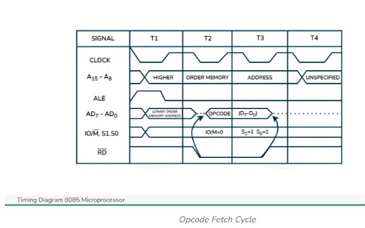
Opcode Fetch Machine Cycle of 8085
Each processor instruction has a one byte opcode.
Operation codes are stored in memory. Thus, the processor performs an opcode load machine cycle to load the opcode from memory.
Thus, each instruction begins with a machine cycle of opcodes.
The time the processor takes to perform an opcode load cycle is 4T.
At this time, the first, 3T-states are used to load the opcode from memory, and the remaining T-states are used for internal opcodes.
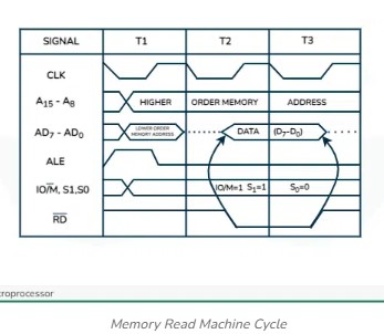
Memory Read Machine Cycle of 8085
A memory read machine cycle is executed by the processor to read a data byte from memory.
The processor takes 3T states to perform this cycle.
Instructions that have more than one byte word will use machine cycle after machine cycle to load the opcode.
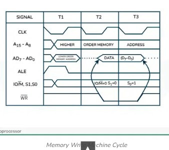
Memory Write Machine Cycle of 8085
A write-to-memory machine cycle is executed by the processor to write a data byte to memory.
The processor takes 3T states to perform this cycle.
Instructions that have more than one byte word will use machine cycle after machine cycle to load the opcode.
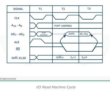
I/O Read Machine Cycle
A reader I/O cycle is performed by the processor to read a data byte from an I/O port or peripheral that is I/O mapped in the system.
The processor needs 3T states to execute this machine cycle.
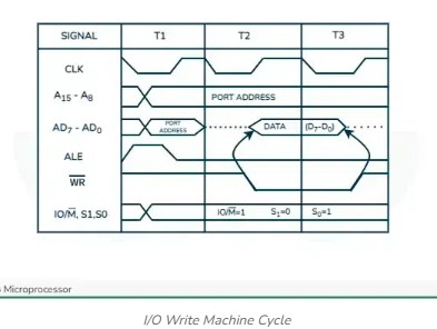
I/O Write Machine Cycle
A writer's I/O cycle is executed by the processor to write a data byte to an I/O port or peripheral that is I/O mapped in the system.
The processor needs 3T states to execute this machine cycle.
Applications 0f 8085
System charts keep track of all changes occurring in the system.
Timelines provide a more accurate representation of physical activity.
The timing table of 8085 instructions graphically represents the time required to execute each instruction.
Timing Diagram is a special form of sequence diagram.
Timing Diagram keep track of every change that occur in the system.
The timing diagram is important for planning the clock frequency of the microprocessor.
The timing diagram helps design memory circuits that meet the required set and hold times during read and write operations.
Instruction set of 8085
- The instruction set of 8085 refers to a collection of commands that control the operations of the microprocessor. These instructions dictate how the processor interacts with the memory, I/O devices, and performs arithmetic or logical operations. Instructions are expressed in machine language, which the processor can interpret directly.
- 8085 microprocessor instructions are grouped into categories based on the function they perform and how they access data. Each instruction includes opcode (operation code) and operands, which specify the task and data involved.
- The instruction set of 8085 microprocessor can be understood through the types of operations it performs:
1. Data Transfer Operations
These instructions move data between registers, memory, or I/O ports. They do not alter the data but copy it from one location to another.
Examples:
MOV B, C: Moves data from register C to register B.
IN 80H: Reads data from input port 80H.
2. Arithmetic Operations
These operations perform arithmetic tasks like addition, subtraction, and increment. The results are stored in the accumulator by default.
Examples:
ADD B: Adds the contents of register B to the accumulator.
DCR B: Decreases the value in register B by 1.
3. Logical Operations
Logical instructions manipulate individual bits and perform operations like AND, OR, and XOR.
Examples:
ANA B: Performs AND operation between accumulator and register B.
CMA: Complements the accumulator contents (bit-wise inversion).
4. Branching Operations
These instructions alter the normal flow of execution. Conditional and unconditional jumps allow for branching based on conditions.
Examples:
JNZ 2050H: Jumps to address 2050H if the zero flag is not set.
CALL 3000H: Calls a subroutine at memory address 3000H.
5. Control Operations
Control instructions handle processor control tasks like enabling/disabling interrupts and halting execution.
Examples:
HLT: Halts the microprocessor operation.
SIM: Sets the interrupt mask to control interrupts.
Applications Instruction Sets of 8085
The 8085 microprocessor found applications in embedded systems, process control equipment, automobiles and many other areas due to its simple yet powerful instruction set. Some common applications include:
Home appliances like washing machines and microwave ovens.
Industrial equipment like motor controllers.
Medical equipment like temperature controllers.
Automotive industry for engine control.
Robotics and 3D printing.
Communication devices like modems.
Security systems.
Educational systems to learn microprocessor programming.
Computer Architecture
Computer Architecture is a blueprint for design and implementation of a computer system. It refers to the overall design of a computer system, including the hardware and software components that make up the system and how they interact with each other.
Computer architecture provides the functional details and behaviour of a computer system. It involves the design of the instruction set, the microarchitecture, and the memory hierarchy, as well as the design of the hardware and software components that make up the system.
Computer Architecture mainly deals with the functional behaviour of a computer system and covers the "What to do?" part.
It gives the functional description of requirements, design, and implementation of the different parts of a computer system.
Computer Organization.
Computer Organization refers to the way in which the hardware components of a computer system are arranged and interconnected. It implements the provided computer architecture and covers the "How to do?" part.
Computer Organization is to be defined after the decision of the computer architecture. It just provides information that how operational attributes of a computer system are linked together and help in realizing the architectural specification of the computer. It involves the design of the interconnections between the various hardware components, as well as the design of the memory and I/O systems.
Difference between Computer Architecture and Computer Organization.
Computer Architecture
They explain what a computer does.
They majorly focus on the functional behaviour of computer systems.
Computer architectures deal with high level design matters.
It comes before computer organisation.
It covers logical functions, such as registers, data types, instruction sets, and addressing modes.
They coordinate between the hardware and software of the system.
Computer Organisation
They explain how a computer actually does it.
They majorly focus on the structural relationship and deep knowledge of the internal working of a system.
They deal with low-level design matters.
It comes after the architecture part.
It covers physical units like peripherals, circuit designs, and adders.
They manage the portion of the network in a system
Von Neumann Architecture
Historically, there have been two types of computers: those that have a very defined function and cannot be programmed, such as calculators, and those that can be programmed (these can be configured to perform a variety of activities, and they store applications).
The contemporary computer is built on John von Neumann’s concept of stored program.
Programs and data are kept in a distinct storage unit called memories in this stored-program approach, and they handle the same.
A computer developed with this design would be considerably easier to reprogram, thanks to this unique notion.
Von-Neumann computer architecture design was proposed in 1945 It’s made up of three fundamental components:
Memory Unit
A memory unit is a collection of storage cells together with associated circuits needed to transfer information in and out of the storage. The memory stores binary information in groups of bits called words. The internal structure of a memory unit is specified by the number of words it contains and the number of bits in each word.
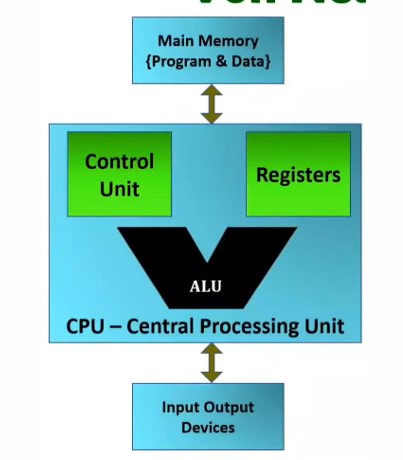
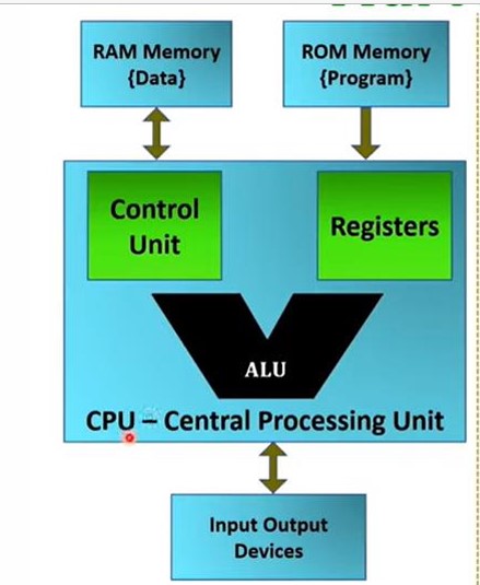
CPU (Central Processing Unit)
The control unit, main memory, and arithmetic-logic unit make up the central processing unit (CPU), which is the most important portion of any digital computer system. The CPU is the computer’s brain, including all of the circuitry required to process input, store data, and generate output. The CPU is always following computer program instructions that instruct it on which information to process as well as how to process it. We couldn’t run applications on a computer without a CPU.
CU (Control Unit)
It is responsible for all processor control signals and timing signals. It governs how data moves throughout the system, directs all input and output flow, and gets code for instructions.
ALU (Arithmetic and Logic Unit)
The arithmetic logic unit (ALU) is the portion of the CPU that handles all of the CPU’s computations, such as addition, subtraction, and comparisons. Also, Logical operations, arithmetic operations, and bit shifting operations are all performed by it.
Registers – Registers refer to high-speed storage areas in the CPU. The data processed by the CPU are fetched from the registers. There are different types of registers used in architecture :-
➢ Accumulator: Stores the results of calculations made by ALU. It holds the intermediate of arithmetic and logical operations. It act as a temporary storage location or device.
➢ Program Counter (PC): Keeps track of the memory location of the next instructions to be dealt with. The PC then passes this next address to the Memory Address Register (MAR).
➢ Memory Address Register (MAR): It stores the memory locations of instructions that need to be fetched from memory or stored in memory.
➢ Memory Data Register (MDR): It stores instructions fetched from memory or any data that is to be transferred to, and stored in, memory.
➢ Current Instruction Register (CIR): It stores the most recently fetched instructions while it is waiting to be coded and executed.
➢ Instruction Buffer Register (IBR): The instruction that is not to be executed immediately is placed in the instruction buffer register IBR
Disadvantages Of Von Neumann Architecture
One of the main limitations is that the shared bus can become a bottleneck if too many devices are connected to it. This can lead to slow performance and reduced scalability.
Additionally, the CPU can only execute one instruction at a time, which can limit the overall speed of the system.
Instruction Cycle
A program consisting of the memory unit of the computer includes a series of instructions.
The program is implemented on the computer by going through a cycle for each instruction.
• The instruction cycle (also known as the Fetch–Decode–Execute cycle or the fetch-execute cycle) is the basic operational process of a computer system.
• The time taken for the execution of an instruction is known as the Instruction Cycle.
• It is the process by which a computer retrieves a program instruction from its memory, determines what actions the instruction describes, and then carries out those actions.
• This cycle is repeated continuously by a computer's central processing unit (CPU), from boot-up until the computer has shut down.
In the basic computer, each instruction cycle includes the following procedures −
➢It can fetch instruction from memory.
➢It is used to decode the instruction.
➢It can read the effective address from memory if the instruction has an indirect address.
➢It can execute the instruction.

Instruction Cycle
➢ Fetch: The CPU fetches, or retrieves, the next instruction from memory.The program counter (PC) holds the address of the current instruction being executed. The CPU reads the instruction located at this address from the memory into its instruction register (IR).
➢ Decode: The fetched instruction is decoded to determine what operation needs to be performed and what data is involved. The CPU interprets the instruction's opcode (operation code) and identifies the specific operation or instruction to be executed.
➢ Execute: After decoding the instruction, the CPU carries out the actual operation specified by the instruction. This might involve performing arithmetic or logical operations, transferring data between registers or memory, or controlling other hardware components. The result of the operation may be stored in registers or memory as needed.
➢ Write Back (optional): In some cases, the CPU needs to write the results of the operation back to memory or registers. For instance, after performing a calculation, the CPU may store the result in a register or update the value in memory.
MACHINE CYCLE
https://nordvpn.com/cybersecurity/glossary/machine-cycle/
https://www.dpgpolytechnic.com/downloads/files/n5c652f73e2e72.pdf
The machine cycle is the most basic operation that a computer performs, and in order to complete
menial tasks such as showing a single character on the screen, the CPU has to perform multiple
cycles. The computer does this from the moment it boots up until it shuts down.It is also known as the instruction cycle.
The steps of a machine cycle are:
Fetch – The control unit requests instructions from the main memory that is stored at amemory’s location as indicated by the program counter (also known as the instructioncounter).
Decode – Received instructions are decoded in the instruction register. This involvesbreaking the operand field into its components based on the instruction’s operation code(opcode).
Execute – This involves the instruction’s opcode as it specifies the CPU operationrequired. The program counter indicates the instruction sequence for computer. Theseinstructions are arranged into the instructions register and as each are executed, itincrements the program counter so that the next instruction is stored in memory.Appropriate circuitry is then activated to perform the requested task. As soon asinstructions have been executed, it restarts the machine cycle that begins the fetch step.
Examples of machine cycle:
Simple processor. Processor used in a calculator might fetch an instruction to add two numbers, decode the instruction to determine the numbers to add, and then execute the addition and display the result.
Basic processor. Processor used in a simple computer might fetch an instruction, decode it to determine the memory address to load from, execute the load, and store the value in a register.
Complex processor. A processor used in a modern computer might fetch an instruction, decode it, execute it, and then perform additional steps such as fetching data from cache or memory, performing pipelining, or handling interrupts.
Data Representation
Data Representation refers to the form in whichdata is stored, processed, and transmitted.
Information handled by a computer is classified as instruction and data. A broad overview of the internal representation of the information is illustrated in figure 3.1. No matter whether it is data in a numeric or non-numeric form or integer, everything is internally represented in Binary. It is up to the programmer to handle the interpretation of the binary pattern and this interpretation is called Data Representation. These data representation schemes are all standardized by international organizations.
Choice of Data representation to be used in a computer is decided by
The number types to be represented (integer, real, signed, unsigned, etc.)
Range of values likely to be represented (maximum and minimum to be represented)
The Precision of the numbers i.e. maximum accuracy of representation (floating point single precision, double precision etc)
If non-numeric i.e. character, character representation standard to be chosen. ASCII, EBCDIC, UTF are examples of character representation standards.
The hardware support in terms of word width, instruction.
Fixed point Number Representation
Fixed point numbers are also known as whole numbers or Integers. The number of bits used in representing the integer also implies the maximum number that can be represented in the system hardware. However for the efficiency of storage and operations, one may choose to represent the integer with one Byte, two Bytes, Four bytes or more. This space allocation is translated from the definition used by the programmer while defining variable as integer short or long and the Instruction Set Architecture.
In addition to the bit length definition for integers, we also have a choice to represent them as below:
Unsigned Integer: A positive number including zero can be represented in this format. All the allotted bits are utilised in defining the number. So if one is using 8 bits to represent the unsigned integer, the range of values that can be represented is 28 i.e. "0" to "255". If 16 bits are used for representing then the range is 216 i.e. "0 to 65535".
Signed Integer: In this format negative numbers, zero, and positive numbers can be represented. A sign bit indicates the magnitude direction as positive or negative. There are three possible representations for signed integers and these are Sign Magnitude format, 1's Complement format and 2's Complement format.
Floating Point Number system
The maximum number at best represented as a whole number is 2'. In the Scientific world, we do come across numbers like Mass of an Electron is 9.10939 x 10⁻³¹ Kg. Velocity of light is 2.99792458 x 10⁸ m/s. Imagine writing the number in a piece of paper without exponent and converting it into binary for computer representation. Sure you are tired!!. It makes no sense to write a number in non readable form or non processable form. Hence we write such large or small numbers using exponent and mantissa. This is said to be Floating Point representation or real number representation.
Rules for Addition & Subtraction Algorithm with Signed-Magnitude Data:
1. When the signs (+,-) of A and B are same, add the two magitudes and attach the sign of A to the result.
2. When the signs (+,-) of A and B are different, compare the magnitudes and subtract the smaller number from the larger.
If A>B, use the sign of A
If A<B, use the sign of B
If A=B, subtract B from A and make the sign positive
Multiplication of Signed Data
Multiplication of two fixed point binary number in signed magnitude representation is done with process of successive shift and add operation.
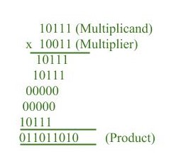
In the multiplication process we are considering successive bits of the multiplier, least significant bit first. If the multiplier bit is 1, the multiplicand is copied down else 0's are copied down. The numbers copied down in successive lines are shifted one position to the left from the previous number. Finally numbers are added and their sum form the product. The sign of the product is determined from the sign of the multiplicand and multiplier. If they are alike, sign of the product is positive else negative.
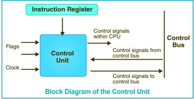
Control unit
The control unit, a vital part of the computer's CPU (central processing unit), orchestrates the processor's operation. The concept of a control unit was first introduced by John von Neumann in his Von Neumann Architecture . The control unit's responsibility is to guide the computer's arithmetic/logic unit, memory, and input and output devices on how to react to the commands given to the processor.
The control unit retrieves internal program commands from the main memory, moves them to the processor instruction register, and produces a control signal based on the register's contents to manage the execution of these commands.
the Working of a CPU Control Unit
A control unit gets data from the user, converts it into control signals, and then passes these signals to the central processor. The computer's processor then guides the connected hardware on the tasks to perform. Since CPU architecture varies from one manufacturer to another, the functions carried out by a control unit in a computer depend on the type of CPU. Examples of devices that require a control unit include:
CPUs or Central Processing Units
GPUs or Graphics Processing Units
The Role of the Control Unit
It manages the flow of data into, out of, and between the different subunits of a processor.
It can interpret commands and instructions.
It regulates the flow of data within the processor.
It can accept external commands or instructions, which it transforms into a series of control signals.
It oversees the multiple execution units of a CPU (such as ALUs, data buffers, and registers).
It also performs various operations, including fetching, decoding, managing execution, and storing results.
Types of Control Unit
Hardwired Control Unit
Micro Programmable Control Unit
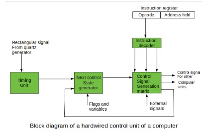
Hardwired Control Unit
The hardwired control unit is a unique form of control signal generation that utilizes Finite State Machines (FSM). This control unit is constructed as a sequential logic circuit, made by physically interconnecting components like flip-flops, gates, and drums to produce the final circuit. Due to its physical construction, it is commonly referred to as a hardwired controller.
The hardwired control unit is a technique used to generate control signals using Finite State Machines (FSM). The control signals necessary for executing instructions in the Hardwired Control Unit are produced by special hardware logic circuits. It is important to note that altering the mechanism of signal production isn't possible without physically modifying the circuit's structure.
Key Features of the Hardwired Control Unit
A Hardwired Control unit is composed of two decoders, a sequence counter, and logic gates.
The instruction register (IR) stores instructions fetched from the memory unit.
The instruction register comprises the operation code, the I bit, and bits 0 through 11.
A 3 x 8 decoder is used to encode the operation code in bits 12 through 14.
The outputs of the decoder are represented by the letters D0 through D7.
The operation code of bit 15 is transferred to a flip-flop denoted by the symbol I.
The control logic gates are programmed with operation codes from bits 0 to 11.
The sequence counter (or SC) has the ability to count from 0 to 15 in binary.
How Does a Hardwired Control Unit Work?
The operation code of an instruction holds the basic data for generating control signals. This operation code is decoded in the instruction decoder, which is a set of decoders that decode various fields of the instruction opcode.
Consequently, only a few of the instruction decoder’s output lines have active signal values. These output lines are connected to the inputs of the matrix, which provides control signals for the computer's executive units. This matrix combines the decoded signals from the instruction opcode with the outputs from the matrix that generates signals indicating consecutive control unit states, along with signals from the external environment, such as interrupt signals.
Benefits of Using a Hardwired Control Unit
The Hardwired Control Unit is fast because it uses combinational circuits to generate signals.
The delay that can occur in the creation of control signals is dependent on the number of gates.
It can be optimized to achieve the fastest mode of operation.
It is faster than a micro-programmed control unit.
Limitations of a Hardwired Control Unit
The design becomes more complex as more control signals need to be generated (requiring more encoders or decoders).
Changes to control signals are challenging as they require reconfiguring the wires in the hardware circuit.
Adding a new feature can be difficult and time-consuming.
Evaluating and fixing flaws in the initial design can be challenging.
It can be somewhat expensive.
Microprogram control unit
A Microprogrammed Control Unit is a unique type of control unit that stores binary control values as words within its memory. It operates by generating specific signal collections at every system clock beat, which in turn, direct the instructions to be executed. Every output signal triggers a micro-operation, like register transfer, which results in specific micro-operations that can be stored within memory due to the sets of control signals.
A programming approach is utilized in the implementation of a microprogrammed control unit. It involves the usage of a program, made up of microinstructions, to execute a series of micro-operations. The control memory of the control unit stores a microprogram, which is composed of these microinstructions. The generation of a set of control signals is contingent on the execution of a microinstruction.
Key Characteristics of a Microprogrammed Control Unit
The control memory address register specifies the address of the microinstruction.
The control memory holds all the control information and is typically considered a ROM.
The control register stores the microinstruction fetched from memory.
A control word in the microinstruction specifies one or several micro-operations for a data processor.
While the micro-operations are being executed, the next address is calculated in the circuit of the next address generator and then transferred to the control address register to read the next microinstruction.
The next address generator, also known as a microprogram sequencer, determines the sequence of addresses retrieved from control memory.
Understanding Instruction Words
In micro-programmed control units, the following instruction words are typically fetched into the instruction register. However, the operation code of each instruction is not directly decoded to enable instant control signal generation; instead, it contains the initial address of a microprogram in the control store.
Utilizing a Single-level Control Store
The instruction opcode from the instruction register is received by the control store address register. This address reads the first microinstruction of a microprogram that interprets the execution of such an instruction to the microinstruction register. The operation element of this microinstruction contains encoded control signals, usually in the form of a few bit fields. These fields are decoded using a set of microinstruction field decoders. Also included in the microinstruction is the address of the next microinstruction in the provided instruction microprogram, along with a control field for controlling the actions of the microinstruction address generator.
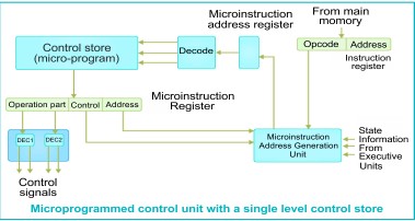
The last-mentioned field determines the addressing mode or addressing operation to be applied to the address encoded in the continuing microinstruction. This address is refined in microinstructions and conditional addressing mode by employing the processor condition flags, which describe the status of calculations in the current program. The last microinstruction in the instruction of the provided microprogram is the microinstruction that fetches the very next instruction to the instruction register from the main memory.
Making use of a Two-level Control Store
A control unit with a two-level control store also contains nano-instruction memory, in addition to the control memory for the microinstructions. In such a control unit, the microinstructions do not include encoded control signals. The operation component of microinstructions contains the address of a word in the nano-instruction memory that carries encoded control signals. The nano-instruction memory stores all combinations of control signals that exist in microprograms that interpret a computer’s entire instruction set, which is written in nano-instructions only once.
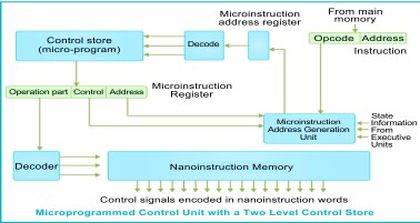
This eliminates the need to store the same operation sections of microinstructions multiple times. In this situation, micro-instruction words can be significantly shorter than in the single level control store, resulting in a significantly smaller microinstruction memory in terms of bits and, consequently, a smaller overall control memory. The control for selecting consecutive microinstructions is stored in the microinstruction memory, whereas those control signals are generated based on nano-instructions. Control signals in nano-instructions are usually encoded using the 1 bit/1 signal technique, which eliminates the need for decoding.
Advantages of a Microprogrammed Control Unit
It enables a systematic design of the control unit.
It’s easier to troubleshoot and modify.
It can maintain the basic structure of the control function.
It simplifies the design of the control unit, making it less expensive and less prone to errors or glitches.
It allows for a methodical and orderly design.
It is used to control software-based functions rather than hardware-based functions.
It’s more flexible.
It can execute complex functions with ease.
Disadvantages of a Microprogrammed Control Unit
Flexibility comes at a higher cost.
It is slower compared to a hardwired control unit.
Control Word:
Control Word: A control word is binary information that makes the general register
organization happen. It is basically a 4-part binary code consisting of SEL A, SEL B, SEL C and
OPR Inputs in the general register organization diagram. The control word is as follows:
Micro program:
A sequence of microinstructions constitutes a microprogram.
Since alterations of the microprogram are not needed once the control unit is in operation,
the control memory can be a read-only memory (ROM).
ROM words are made permanent during the hardware production of the unit.
The use of a micro program involves placing all control variables in words of ROM for
use by the control unit through successive read operations.
The content of the word in ROM at a given address specifies a microinstruction.
Control Memory
The control memory address register specifies the address of the micro-instruction, and the control data register holds the micro-instruction read from memory. The control memory is assumed to be a ROM (Read Only Memory), which stores all control information.
The next address generator is sometimes called a micro-programed sequencer, as it determines the address sequence that is read from control memory.
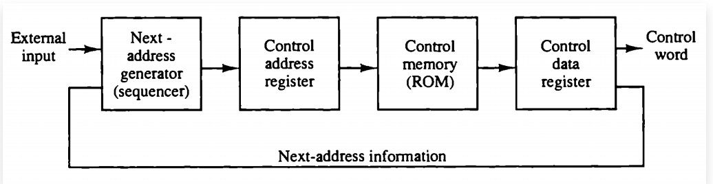
The micro-instruction contains a control word that specifies one or more micro-operations for the data processor.
The address sequencing capabilities required in a control memory are:
Incrementing of the control address register.
Unconditional branch or conditional branch, depending on status bit conditions.
A mapping process from the bits of the instruction to an address for control memory.
A facility for subroutine call and return.
Control Address Register (CAR)
A Control Address Register (CAR) is a specialized register used in computer architecture, particularly in the context of memory management and control. Its primary purpose is to hold the address of a memory location that is being accessed or manipulated by the processor. Here’s a more detailed explanation:
Key Functions of a Control Address Register:
Address Storage: The CAR stores the address of the next instruction to be executed or the address of data to be read or written in memory.
Memory Management: In systems with virtual memory, the CAR can be used to hold the virtual address that needs to be translated to a physical address by the Memory Management Unit (MMU).
Control Operations: The CAR may also be involved in control operations, directing the flow of data between the CPU and memory or between different components of the system.
Efficiency: By using a dedicated register for address control, the CPU can perform memory operations more efficiently, reducing the need for multiple cycles to fetch and decode addresses.
Context of Use:
The CAR is often utilized in the context of specific architectures or systems, such as microcontrollers, embedded systems, or more complex CPUs where memory management is critical.
It plays a role in ensuring that the processor accesses the correct memory locations, particularly in systems that implement paging or segmentation.
In summary, the Control Address Register is a crucial component in managing how a processor interacts with memory, ensuring efficient data retrieval and instruction execution.
Address Sequencing
In computer architecture, address sequencing is the process of generating a sequence of memory addresses.
The control memory is used to store the microinstructions in groups. Here each group is used to specify a routine. The control memory of each computer has the instructions which cơ tain their micro-programs routine. These micro-programs are used to generate the micro-operations that will be used to execute the instructions. Suppose the address sequencing of control memory is controlled by the hardware. In that case, that hardware must be capable to branch from one routine to another routine and also able to apply sequencing of microinstructions within a rou ine. When we try to execute a single instruction of computer, the control must undergo the following steps:
When the power of a computer is turned on, we have to first load an initial address into the CAR (control address register). This address can be described as the first microinstruction address. With the help of this address, we are able to activate the instruction fetch routine.
Then, the control memory will go through the routine, which will be used to find out the effective address of operand.
In the next step, a micro-operation will be generated, which will be used to execute the instruction fetched from memory.
We are able to transform the bits of instruction code into an address with the help of control memory where routine is located. This process can be called the mapping process. The control memory required the capabilities of address sequencing, which is described as follows:
On the basis of the status bit conditions, the address sequencing selects the conditional branch or unconditional branch.
Addressing sequence is able to increment the CAR (Control address register).
It provides the facility for subroutine calls and returns.
A mappings process is provided by the addressing sequence from the instruction bits to a control memory address.
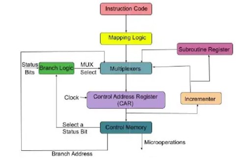
In the above diagram, we can see a block diagram of a control memory and associative hardware, which is required for selecting the address of next microinstruction. The microinstruction is used to contain a set of bits in the control memory. With the help of some bits, we are able to start the micro-operations in a computer register. The remaining bits of microinstruction are used to specify the method by which we are able to obtain the next address.
In this diagram, we can also see that the control address register are able to recover their address with the help of four different directions. The CAR is incremented with the help of incrementer and then chooses the next instruction. The branching address will be determined in the multiple fields of microinstruction so that they can provide results in branching.
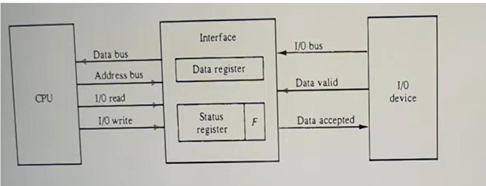
Input-Output Interface
- Input-Output Interface is used as a method which helps in transferring of information between the internal storage devices i.e. memory and the external peripheral device . A peripheral device is that which provide input and output for the computer, it is also called Input-Output devices. For Example: A keyboard and mouse provide Input to the computer are called input devices while a monitor and printer that provide output to the computer are called output devices. Just like the external hard-drives, there is also availability of some peripheral devices which are able to provide both input and output.
- In micro-computer base system, the only purpose of peripheral devices is just to provide special communication links for the interfacing them with the CPU. To resolve the differences between peripheral devices and CPU, there is a special need for communication links.
Functions of Input-Output Interface:
It is used to synchronize the operating speed of CPU with respect to input-output devices.
It selects the input-output device which is appropriate for the interpretation of the input-output signal.
It is capable of providing signals like control and timing signals.
In this data buffering can be possible through data bus.
There are various error detectors.
It converts serial data into parallel data and vice-versa.
It also convert digital data into analog signal and vice-versa.
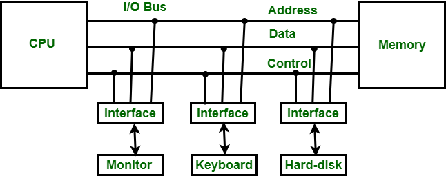
I/O Bus and Interface Modules or Input-Output Interface
Input-output interface provides a method for transferring information between internal storage and external I/O devices. Peripherals connected to a computer need special communication links for interfacing them with the central processing unit. The major differences are:
1. Peripherals are electromechanical and electromagnetic devices and their manner of operation is different from the operation of the CPU and memory, which are electronic devices. Therefore, a conversion of signal values may be required.
2. The data transfer rate of peripherals is usually slower than the transfer rate of the CPU,and consequently, a synchronization mechanism may be needed.
3. Data codes and formats in peripherals differ from the word format in the CPU and memory.
4. The operating modes of peripherals are different from each other and each must becontrolled so as not to disturb the operation of other peripherals connected to the CPU.
A typical communication link between the processor and several peripherals is shown in Fig.36. The I/O bus consists of data lines, address lines, and control lines. The magnetic disk, printer, and terminal are employed in practically any general-purpose computer. The interface selected responds to the function code and proceeds to execute it. The function code is referred to as an I/O command and is in essence an instruction that is executed in the interface and its attached peripheral unit.
There are three ways that computer buses can be used to communicate with memory and I/O:
1. Use two separate buses, one for memory and the other for I/O.
2. Use one common bus for both memory and I/O but have separate control lines for each.
3. Use one common bus for memory and I/O with common control lines.
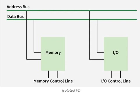
Isolated I/O
In Isolated I/O, the CPU uses the same buses (wires) to talk to both memory and I/O devices, but it has separate control signals to tell whether it’s dealing with memory or an I/O device.
I/O devices have special addresses called ports.
When the CPU wants to communicate with an I/O device:
It puts the port address on the address bus.
It uses special control lines like I/O Read or I/O Write.
Then data is sent or received using the data bus.
As memory and I/O have separate address spaces, it’s called Isolated I/O. Also, the CPU uses different instructions for memory and I/O (like IN and OUT for I/O).
Applications of Isolated I/O
Embedded Systems: Isolated I/O is widely used in embedded systems where strict separation between the CPU and peripherals is essential. This includes applications like industrial control systems, robotics, and automotive electronics. Isolation helps ensure that faults or malfunctions in peripheral devices do not compromise the stability of the entire system.
Microcontrollers: Microcontrollers often use isolated I/O to interface with various peripherals such as sensors, actuators, and displays. Each device is assigned a unique I/O port, allowing the microcontroller to communicate with multiple peripherals independently and efficiently.
Real-Time Systems: In real-time systems, where precise timing and predictable behavior are critical, isolated I/O is preferred. It allows for strict control over timing and synchronization of external events, helping the system maintain reliable and deterministic performance.
Advantages of Isolated I/O
Large I/O Address Space: Isolated I/O allows for a larger I/O address space because I/O devices have their own separate address space, independent of the system memory.
Greater Flexibility: It offers greater flexibility, as I/O devices can be added or removed without affecting the memory address space.
Improved Reliability: Since I/O devices do not share the same address space as memory, failures in I/O devices are less likely to affect the memory or other devices, improving system reliability.
Disadvantages of Isolated I/O
Slower I/O Operations: I/O operations may be slower because isolated I/O requires special instructions, which add extra processing steps.
More Complex Programming: Programming becomes more complex due to the need for dedicated I/O instructions, such as IN and OUT, which are separate from standard memory instructions.
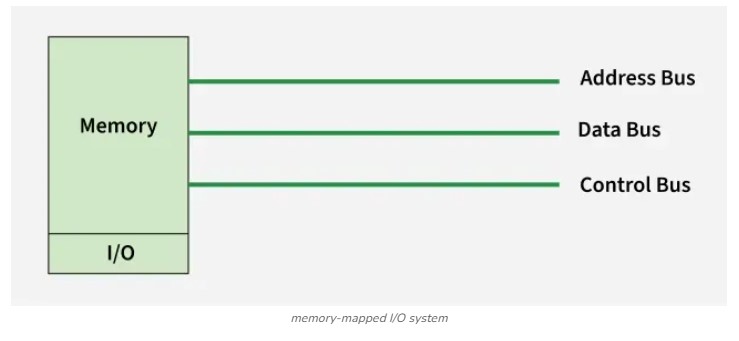
Memory Mapped I/O
In a memory-mapped I/O system, there are no special input or output instructions. Instead, the CPU uses the same instructions it uses for memory (like LOAD and STORE) to access I/O devices.
Each I/O device is assigned a specific address in the regular memory address space.
Devices are connected through interface registers, which act like memory locations.
When the CPU wants to read from or write to an I/O device, it accesses the corresponding address, just like it would access a memory word.
These interface registers respond to normal read/write operations as if they were memory cells.
This design allows I/O and memory to be treated uniformly, simplifying programming and hardware design.
Applications of Memory-Mapped I/O
Graphics Processing: Memory-mapped I/O is widely used in graphics cards to provide fast access to frame buffers and control registers. Graphics data is mapped directly to memory, allowing the CPU to interact with the graphics hardware as if it were accessing normal memory. This enables efficient rendering and display operations.
Network Communication: Network Interface Cards (NICs) often use memory-mapped I/O to manage data transfer between the system memory and the network. The NIC’s control and status registers are mapped to specific memory addresses, allowing the CPU to efficiently control and monitor network operations.
Direct Memory Access (DMA): DMA controllers use memory-mapped I/O to enable high-speed data transfers between I/O devices and system memory without involving the CPU. By mapping DMA control registers to memory, devices can transfer data directly, improving system performance and reducing CPU load.
Advantages of Memory-Mapped I/O
Faster I/O Operations: Memory-mapped I/O allows the CPU to access I/O devices using the same mechanism and speed as regular memory access. This results in faster I/O operations compared to isolated I/O.
Simplified Programming: Since the same instructions are used for both memory and I/O operations, programming becomes easier. Developers do not need to learn or use special I/O instructions, reducing complexity.
Efficient Use of Address Space: Memory-mapped I/O enables I/O devices to share the same address space as memory. This can make the system more efficient, especially in systems with a unified memory model.
Disadvantages of Memory-Mapped I/O
Limited I/O Address Space: Because memory and I/O devices share the same address space, the number of available addresses for I/O devices is limited. This can be a problem in systems with many peripherals.
Potential Performance Issues: If an I/O device responds slowly, it may delay the CPU when accessing that memory-mapped region. This can affect overall system performance, especially in time-sensitive tasks.
Differences between memory mapped I/O and isolated I/O
Let us see the difference between the memory mapped I/O and isolated I/O in the below table:
Isolated I/O
Memory and I/O have separate address spaces
All addresses can be used for memory
Separate instructions for I/O and memory read/write operations
I/O addresses are called ports
More efficient due to separate control lines and buses
Larger hardware due to additional buses and logic
More complex requires separate logic for I/O and memory
Memory-Mapped I/O
Memory and I/O share the same address space
Some address space is used for I/O, reducing memory space
Same instructions are used for both I/O and memory
Regular memory addresses are used for both memory and I/O
Slightly less efficient due to shared resources
Smaller hardware as fewer buses are needed
Simpler design I/O is handled like memory
Programmed I/O
• Programmed I/O instructions are the result of I/O instructions written in a computer program. Each data item transfer is initiated by the instruction in the program.
• Usually the program controls data transfer to and from CPU and peripheral. Transferring data under programmed I/O requires constant monitoring of the peripherals by the CPU.
• It is the responsibility of the processor to control the transfer from I/O to main memory as input and from main memory to I/O as output.
•To overcome the difference in the speed of the processor and I/O device a mechanism must be implemented to synchronize the transfer of data between the processor and I/O modules. This is we require programmed I/O
• When the processor is executing a program and encounters an instruction relating to input/output, it executes that instruction by issuing a command to the appropriate input/output module.
• With the programmed input/output, the input/output module will perform the required action and then set the appropriate bits in the input/output status register.
• The input/output module takes no further action to alert the processor. In particular it doesn't interrupt the processor. Thus, it is the responsibility of the BUS Device CPU Memory I/O DMA processor to check the status of the input/output module periodically, until it finds that the operation is complete.
Disadvantages
• In the programmed I/O method the CPU stays in the program loop until the I/O unit indicates that it is ready for data transfer. This is time consuming process because it keeps the processor busy needlessly.
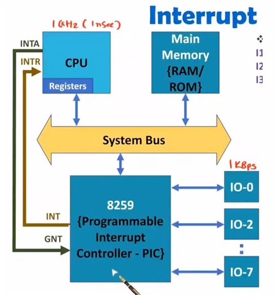
Interrupt-driven I/O
It is such type of I/O programming in which the processor does not wait until the I/O operation is completed. The processor performs other tasks while the I/O operation is being performed.
When the I/O operation is completed, the I/O module interrupts the processor letting the processor know the operation is completed. Its module is faster than the programmed I/O module.
The processor actually starts the I/O device and instructs it to generate and send an interrupt signal when the operation is finished. This is achieved by setting an interrupt enabled bit in the status register.
This technique requires an interrupt for each character that is written or read. It is an expensive business to interrupt a running process as it requires saving context.
It requires additional hardware such as a PIC controller chip. It is fast and efficient.
The system's performance is improved and enhanced.
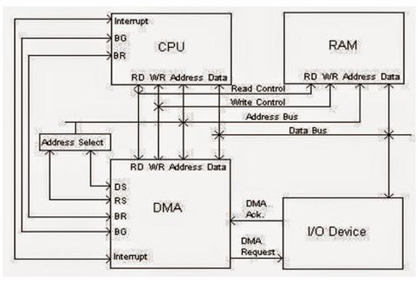
Direct memory access (DMA)
DMA (Direct memory access) is the special feature within the computer system that transfers the data between memory and peripheral devices(like hard drives) without the intervention of the CPU.
The process is managed by a chip known as a DMA controller
Working of DMA Controller
• DMA controller must share the bus with the processor to make the data transfer.
• The device that holds the bus at a given time is called bus master.
When an I/O device wants to initiate the transfer then it sends a DMA request signal to the DMA controller, for which the controller acknowledges if it is free If the DMA controller is free, it requests the control of bus from the processor by raising the bus request signal.
• Processor grants the bus to the controller by raising the bus grant signal, now DMA controller is the bus master.
• The processor initiates the DMA controller by sending the memory addresses, number of blocks of data to be transferred and direction of data transfer.
• After assigning the data transfer task to the DMA controller, instead of waiting ideally till completion of data transfer, the processor resumes the execution of the program after retrieving instructions from the stack.
• DMA controller now has the full control of buses and can interact directly with memory and I/O devices independent of CPU.
• It makes the data transfer according to the control instructions received by the processor.
• After completion of data transfer, it disables the bus request signal and CPU disables the bus grant signal thereby moving control of buses to the CPU.
Harvard architecture
Harvard architecture is a type of computer architecture that has separate memory spaces for instructions and data. It was developed at Harvard University in the 1930s, and it is named after this institution.
In a Harvard architecture system, the CPU accesses instruction and data memory spaces separately, which can lead to improved performance.
Overall, Von Neumann architecture is more flexible and easier to program, whereas Harvard architecture is more efficient and better suited for embedded systems that require high performance and reliability.
Components:
✓CPU: The central processing unit performs all the calculations and operations required to execute instructions.
✓Instruction memory: This memory holds instructions that the CPU needs to execute. It is typically implemented as read-only memory (ROM) or flash memory.
✓Data memory: This memory holds data that the CPU needs to perform computations. It is typically implemented as random access memory (RAM).
✓Input/output (I/O) devices: These devices are used to communicate with the outside world. Examples include keyboards, displays, and printers.
✓System bus: The system bus is a collection of wires that connect the CPU, instruction memory, data memory, and
I/O devices. It is used to transmit data, instructions, and control signals between these components.
Advantages Of Harvard Architecture
✓The CPU can access both instruction and data memory simultaneously.
✓This can lead to improved performance because the CPU does not have to switch between memory spaces as often as in a Von Neumann architecture.
✓Additionally, because the instruction memory is typically implemented as ROM or flash memory,it is non-volatile, meaning that it does not lose its contents when power is turned off.
✓This makes it well-suited for embedded systems that need to operate without a constant power source.
Disadvantages Of Harvard Architecture
✓As the CPU accesses instruction and data memory separately, it can be more difficult to write programs that require the CPU to modify its own code.
✓Additionally, because the instruction and data memories are separate, it can be more difficult to share data between different parts of a program.
Difference between Von Neumann Architecture & Harvard Architecture
- Memory:- Single memory for instructions and data Separate memory for instructions and data
- Access:- CPU accesses instructions and data through a shared bus CPU accesses instruction and data memory spaces separately
- Performance:- Can become a bottleneck if too many devices are connected to the shared bus
- Improved performance:- because the CPU can access both instruction and data memory simultaneously
- Modification:- Easier to modify programs as instructions and data are stored in the same memory
- More difficult to modify programs that require the CPU to modify its own code
- Data sharing:- Easy to share data between different parts of a program
- More difficult to share data between different parts of a program
- Applications:- Suitable for general-purpose computing where flexibility is required
- Suitable for embedded systems where performance is critical, and code is not frequently modified
RISC Architecture
RISC stands for Reduced Instruction Set Computer Processor, a microprocessor architecture with a simple collection and highly customized set of instructions.
It is built to minimize the instruction execution time by optimizing and limiting the number of instructions. It means each instruction cycle requires only one clock cycle, and each cycle contains three parameters: fetch, decode and execute.
The RISC processor is also used to perform various complex instructions by combining them into simpler ones. RISC chips require several transistors, making it cheaper to design and reduce the execution time for instruction.
Examples of RISC processors are SUN's SPARC, PowerPC, Microchip PIC processors, RISC-V
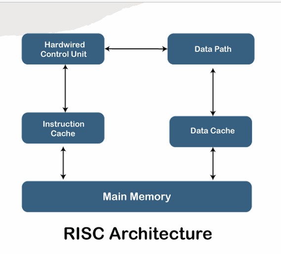
Characteristics of RISC:
1. It has simpler instructions and thus simple instruction decoding.
2. More general-purpose registers.
3. The instruction takes one clock cycle in order to get executed.
4. The instruction comes under the size of a single word.
5. Pipeline can be easily achieved.
6. Few data types.
7. Simpler addressing modes.
CISC
The CISC architecture comprises a complex instruction set. A CISC processor has a variable-length instruction format. In this processor architecture, the instructions that require register operands can take only two bytes.
In a CISC processor architecture, the instructions which require two memory addresses can take five bytes to comprise the complete instruction code. Therefore, in a CISC processor, the execution of instructions may take a varying number of clock cycles. The CISC processor also provides direct manipulation of operands that are stored in the memory.
The primary objective of the CISC processor architecture is to support a single machine instruction for each statement that is written in a high-level programming language.
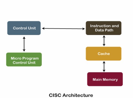
Characteristics of CISC:
• The length of the code is short, so it requires very little RAM.
• CISC or complex instructions may take longer than a single clock cycle to execute the code.
• Less instruction is needed to write an application.
• It provides easier programming in assembly language.
• Support for complex data structure and easy compilation of high-level languages.
• It is composed of fewer registers and more addressing nodes, typically 5 to 20.
• Instructions can be larger than a single word.
• It emphasizes the building of instruction on hardware because it is faster to create than the software.
Difference Between RISC and CISC
RISK
1. It stands for Reduced Instruction Set Computer.
2.It is a microprocessor architecture that uses a small instruction set of uniform length.
3.These simple instructions are executed in one clock cycle.
4. These chips are relatively simple to design.
5. They are inexpensive.
6. Examples of RISC chips include SPARC, POWER PC.
7. It has a smaller number of instructions.
8. It has fixed-length encodings for instructions.
9. Simple addressing formats are supported.
10. It doesn't support arrays. It has a large number of instructions.
11. It doesn't use condition codes.
12. Registers are used for procedure arguments and return addresses.
CISC
It stands for Complex Instruction Set Computer.
This offers hundreds of instructions of different sizes to the users.
This architecture has a set of special purpose circuits which help execute the instructions at a high speed.
These chips are complex to design.
Examples of CISC include Intel architecture, AMD.
They are relatively expensive.
It has more instructions.
It has variable-length encodings of instructions.
The instructions interact with memory using complex addressing modes.
It supports arrays.
Condition codes are used.
The stack is used for procedure arguments and return addresses.


%20(3).png)
Comments
Post a Comment